Difference between revisions of "10334"
(→FPPGA vs. CPU signals) |
(→discussion) |
||
| (One intermediate revision by the same user not shown) | |||
| Line 76: | Line 76: | ||
Wensai | Wensai | ||
| + | |||
| + | === discussion === | ||
| + | Lets's move discussion to "discussion" tab ( [[Talk:10334]] ) | ||
| + | |||
| + | (you may delete this section after you see it) | ||
| + | |||
| + | Andrey | ||
Latest revision as of 21:09, 23 September 2005
Discussion on russian 10334.Ru
In my board 10332 use this net

1. EXT_SCL	-	MISO
2. EXT_SDA	-	MOSI
3. EXT_RST	-	RESET
4. EXT_CLK	-	XTAL1
5. EXT_EXPOS	-	SCK
Your dauther board is incompatible with too. Ok.
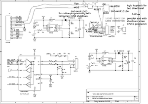
In your shematic we can get high speed 12Mbps USB, but for programming lens control board, need to set jumper. May be use single gate logic from Texace Instrument for generate #RESET for the lens control board combination of nets #OE and Vpo. When #OE set to high level, the USB transiever is shutdown, when Vpo set to high level logic gate generate #RESET for our lens control board. We may use for example SN74AUP1G00 from Texace Instrument.
Master is the CPU board, MOSI (Master Output, Slave Input), but you connect MOSI net to INPUT pin in the CPU. The serial1 pins is not two directional, it is unidirectional, see datasheet of the CPU.
 master		        	Wensai		CPU
 out SCK			RXD1		T17 in
 out MOSI			CTS1		V19 in
 in  MISO			TXD1		U19 out
I think these connections are correct
   master	CPU	        loop
   out SCK	RTS1 W20 out
   out MOSI	TXD1 U19 out     *
   in MISO	RXD1 T17 in
via external single gate element connect out MOSI with in MISO for two-direction 1-Wire protocol and for shutdown the loopback when lens board is programming mode.(SN74AUP1G126).
You can see your shematic with my bugfix follow
FPGA vs. CPU signals
I think that it is better to use FPGA signals for the implementation of USB so we will have the freedom to start with pure software USB implementation but move it to FPGA later. Or even make it something intermediate - partially in FPGA - partially in software.
Programming of the lens adapter is not a frequent and a speed-critical operation, so we can use CPU pins for that purpose. And that operation may even require a special adapter - or what is the sense to use a single-wire interface if we have to connect programming pins also. So there is an option that finally we will have just 2 spring permanently mounted in the camera contacts for the lens adapter and additional small regular connector on the 10334 board so we can connect the lens adapter for programming to that interface (opening the camera). So it is possible to have a jumper on the cable side of the connector that will indicate that the system is in adapter programming mode.
So the 10334 board will have:
- an external USB connector;
- a 16-pin inter-board connector;
- 2 pin connector for the single-wire interface;
- 6(?) pin connector for programming of lens adapter (cable side will have a jumper between 2 pins)
Andrey
Question
Why Wensai`s shematic with my changes is bad?
Dmitry.
Free Software and Open Hardware. Elphel, Inc., 2005
My idea
When programming of lens adapter use the jump wire ,at the time ,can not use USB master port.
Lens adapter have programmed,the jump wire open.we can control the lens adapter overpass other 4 single-wires
(Only can not reset the microprocessor by hardware,but the microprocessor can reset by soft.)
Wensai
discussion
Lets's move discussion to "discussion" tab ( Talk:10334 )
(you may delete this section after you see it)
Andrey
