Difference between revisions of "103696"
m |
|||
| (9 intermediate revisions by 2 users not shown) | |||
| Line 1: | Line 1: | ||
== 103696 - Serial GPS Adapter Board with Synchro Input == | == 103696 - Serial GPS Adapter Board with Synchro Input == | ||
| − | [[Image:103696.jpeg|frame|[[Media: | + | [[Image:103696.jpeg|frame|[[Media:103696a.pdf|103696 Circuit Diagram, Parts List, PCB layout]] [[Media:103696a_gerber.tar.gz|103696A Gerber files]]]] |
=== Description === | === Description === | ||
103696 is an adapter board used with the [[10369]] interface board to connect [http://en.wikipedia.org/wiki/NMEA_0183 NMEA 0183] serial GPS devices to the [[353 | Elphel Model 353 camera]]. | 103696 is an adapter board used with the [[10369]] interface board to connect [http://en.wikipedia.org/wiki/NMEA_0183 NMEA 0183] serial GPS devices to the [[353 | Elphel Model 353 camera]]. | ||
| Line 9: | Line 9: | ||
The board uses two alternative connectors to the GPS device: | The board uses two alternative connectors to the GPS device: | ||
| − | *standard (with | + | *standard (with extra connections for GPS power and synchro pulse) for RS-232 9-pin DSUB (male) or |
*8-pin low profile Hirose connector | *8-pin low profile Hirose connector | ||
First option is used when the board is mounted on the camera body and the connector extends outside for the external GPS, the second - when the GPS is mounted inside the camera body. In that case the DSUB mounting holes are used to mount the 103696 adapter board. | First option is used when the board is mounted on the camera body and the connector extends outside for the external GPS, the second - when the GPS is mounted inside the camera body. In that case the DSUB mounting holes are used to mount the 103696 adapter board. | ||
| Line 47: | Line 47: | ||
==== J2 - DSUB-9 (male) for external GPS connection ==== | ==== J2 - DSUB-9 (male) for external GPS connection ==== | ||
{| class="wikitable" style="background:#fcfcfc; " border="1" | {| class="wikitable" style="background:#fcfcfc; " border="1" | ||
| − | |+ connector to the | + | |+ connector to the external GPS device |
|- | |- | ||
! Pin !! Signal !! Notes | ! Pin !! Signal !! Notes | ||
| Line 57: | Line 57: | ||
| 3 || TXD || Serial data signal to the GPS, output | | 3 || TXD || Serial data signal to the GPS, output | ||
|- | |- | ||
| − | | 4 || GPSPWR || GPS 3.3V power (non-standard for RS-232), output | + | | 4 || GPSPWR || GPS 3.3V power (non-standard for RS-232), output (may be changed to 5.0V on the 103696 board) |
|- | |- | ||
| 5 || GND || ground | | 5 || GND || ground | ||
| Line 75: | Line 75: | ||
==== J3 - Internal connector for the GPS ==== | ==== J3 - Internal connector for the GPS ==== | ||
{| class="wikitable" style="background:#fcfcfc; " border="1" | {| class="wikitable" style="background:#fcfcfc; " border="1" | ||
| − | |+ connector to the | + | |+ connector to the internal GPS device |
|- | |- | ||
! Pin !! Signal !! Notes | ! Pin !! Signal !! Notes | ||
| Line 85: | Line 85: | ||
| 3 || TXD || Serial data signal to the GPS, output | | 3 || TXD || Serial data signal to the GPS, output | ||
|- | |- | ||
| − | | 4 || GPSPWR || GPS 3.3V power (non-standard for RS-232), output | + | | 4 || GPSPWR || GPS 3.3V power (non-standard for RS-232), output (may be changed to 5.0V on the PCB) |
|- | |- | ||
| 5 || GND || ground | | 5 || GND || ground | ||
| Line 101: | Line 101: | ||
==== J4 - Auxiliary GPS Power ==== | ==== J4 - Auxiliary GPS Power ==== | ||
{| class="wikitable" style="background:#fcfcfc; " border="1" | {| class="wikitable" style="background:#fcfcfc; " border="1" | ||
| − | |+ | + | |+ Auxiliary power input |
|- | |- | ||
! Pin !! Signal !! Notes | ! Pin !! Signal !! Notes | ||
|- | |- | ||
| − | | 1 || GPSPWR || optional external power | + | | 1 || GPSPWR || optional external power for the GPS device |
|- | |- | ||
| 2 || GND || ground | | 2 || GND || ground | ||
| Line 111: | Line 111: | ||
|} | |} | ||
---- | ---- | ||
| + | |||
| + | |||
| + | ==Set 3.3V or 5V power to the GPS receiver== | ||
| + | The power voltage level is set with JP4 and JP5 jumpers. | ||
| + | {| | ||
| + | |- | ||
| + | | [[File:103696 jumpers.jpeg|300px|thumb|JP4 & JP5 jumpers]] | ||
| + | |} | ||
| + | {| class="wikitable" style="background:#fcfcfc; " border="1" | ||
| + | |- | ||
| + | !Power !! JP4 !! JP5 | ||
| + | |- | ||
| + | | 3.3V || disconnected || connected | ||
| + | |- | ||
| + | | 5V || connected || disconnected | ||
| + | |} | ||
| + | |||
| + | ==Garmin GPS 18x LVC & GPS 18x-5Hz wiring== | ||
| + | {| | ||
| + | |[[File:Garmin gps18x wiring.jpeg|500px]] | ||
| + | |} | ||
Latest revision as of 09:56, 17 July 2013
Contents
103696 - Serial GPS Adapter Board with Synchro Input
Description
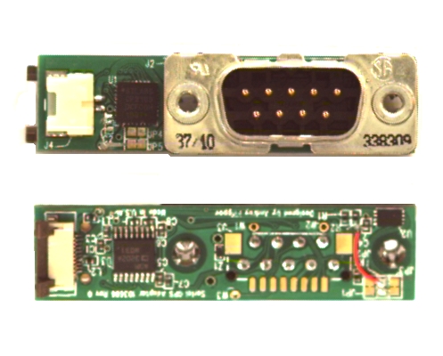
103696 is an adapter board used with the 10369 interface board to connect NMEA 0183 serial GPS devices to the Elphel Model 353 camera.
Adapter provides 3.3V/5.0V (jumper selectable) power to the GPS device, communicates with it over RS-232 (+/-5V) TxD/RxD lines and uses optional synchronization pulse (usually 1pps) from the device. It includes USB-to-Seraial converter chip that allows full communication with the GPS device using the camera software, additionally the RxD signal is fed to the camera FPGA, decoded and logged in the camera sytem memory buffer - together with the optional IMU data, each message with the microsecond resolution timestamp. The source of the timestamp even is selectable among synchronization pulse from the GPS (either polarity), the start bit of the first NMEA sentence afther the pause or the start of each individual NMEA sentence. Current FPGA code allows programming of up to 4 different NMEA sentences that are recognized, decoded and logged.
Connectors
The board uses two alternative connectors to the GPS device:
- standard (with extra connections for GPS power and synchro pulse) for RS-232 9-pin DSUB (male) or
- 8-pin low profile Hirose connector
First option is used when the board is mounted on the camera body and the connector extends outside for the external GPS, the second - when the GPS is mounted inside the camera body. In that case the DSUB mounting holes are used to mount the 103696 adapter board.
J1 - to the 10369 board
| Pin | Signal | Notes |
|---|---|---|
| 1 | VP33IN | +3.3V power input |
| 2 | IPULSE1SEC | GPS synchro pulse to FPGA, output |
| 3 | IRXD | GPS data line converted to TTL levels for FPGA, output |
| 4 | SDA | i2c SDA |
| 5 | SCL | i2c SCL |
| 6 | GND | ground |
| 7 | VP5IN | USB +5V power |
| 8 | DM | USB data - |
| 9 | DP | USB data + |
| 10 | GND | ground |
J2 - DSUB-9 (male) for external GPS connection
| Pin | Signal | Notes |
|---|---|---|
| 1 | PULSE1SEC | GPS synchro pulse (non-standard for RS-232), input |
| 2 | RXD | Serial data signal from the GPS, input |
| 3 | TXD | Serial data signal to the GPS, output |
| 4 | GPSPWR | GPS 3.3V power (non-standard for RS-232), output (may be changed to 5.0V on the 103696 board) |
| 5 | GND | ground |
| 6 | DSR | unused, connected to wirepad W1 |
| 7 | RTS | RS-232 RTS signal, output |
| 8 | CTS | RS-232 CTS signal, input |
| 9 | RI | unused, connected to wirepad W2 |
J3 - Internal connector for the GPS
| Pin | Signal | Notes |
|---|---|---|
| 1 | PULSE1SEC | GPS synchro pulse (non-standard for RS-232), input |
| 2 | RXD | Serial data signal from the GPS, input |
| 3 | TXD | Serial data signal to the GPS, output |
| 4 | GPSPWR | GPS 3.3V power (non-standard for RS-232), output (may be changed to 5.0V on the PCB) |
| 5 | GND | ground |
| 6 | GP1 | unused, connected to wirepad W3 |
| 7 | RTS | RS-232 RTS signal, output |
| 8 | CTS | RS-232 CTS signal, input |
J4 - Auxiliary GPS Power
| Pin | Signal | Notes |
|---|---|---|
| 1 | GPSPWR | optional external power for the GPS device |
| 2 | GND | ground |
Set 3.3V or 5V power to the GPS receiver
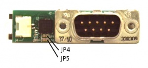
The power voltage level is set with JP4 and JP5 jumpers.
| Power | JP4 | JP5 |
|---|---|---|
| 3.3V | disconnected | connected |
| 5V | connected | disconnected |
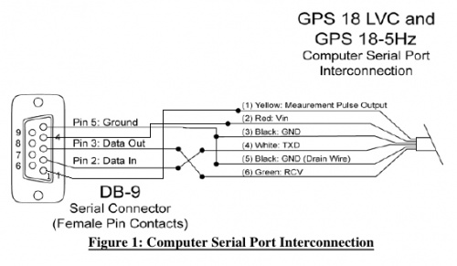
Garmin GPS 18x LVC & GPS 18x-5Hz wiring

|

