Difference between revisions of "10349"
(→Body of camera for developers) |
|||
| Line 121: | Line 121: | ||
[[Image:Developer-body-1_3.png|thumb|Body for developers kit other of A]] | [[Image:Developer-body-1_3.png|thumb|Body for developers kit other of A]] | ||
| + | === Another version of a "developer" camera body === | ||
| + | Here are the rendered 3d-image and the source files [[http://wiki.elphel.com/index.php?title=Image:Assembly200709-developer_af01.png]] | ||
Revision as of 12:18, 26 October 2007
Russia page 10349.Ru
Contents
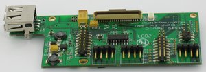
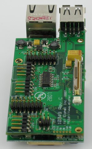
[hide]Interface board.
- serial port
- 4 ports USB hub with 3 internal, 1 external USB ports
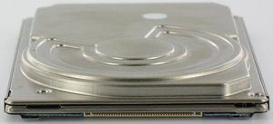
- IDE port for the 1.8" hard drive with ZIF Flat cable
- 2 socket for external usermade board
- some points for soldering wires directly to board (from external board to 10349 for example), easy hardware developing.
Connector pinouts
 internal USB2, USB3, USB4
   1 - power
   2 - D-
   3 - D+
   4 - GND
 J7 is the serial port
   1 - RX
   2 - TX
   3 - CTS
   4 - RTS
   5 - GND
   6 - removed, used as key
 J7 pin layout (1 is marked)

(GND)       (RX)
     5  3  1
     6  4  2
            (TX)
J4 for connect external boards. All wires of J4 connected to the solder pads. For make connection via wires.
 J5 for connect external boards
   1 - EXT0 (FPGA IO signal)
   2 - EXT1 (FPGA IO signal)
   3 - EXT2 (FPGA IO signal)
   4 - EXT3 (FPGA IO signal)
   5 - EXT4 (FPGA IO signal)
   6 - GND
   7 - EXT5 (FPGA IO signal)
   8 - GND
   9 - +3.3V
   10 - +3.3V
   11 - CTS (TTL level)
   12 - RTS (TTL level)
   13 - RX (TTL level)
   14 - TX (TTL level)
   15 - not connected
   16 - not connected
Power description
It has DC-DC converter 3.3V->5V 1.5A. Each USB port has current limit to 300mA. Each port is overcurrent protected via USB power distributed systems. Use both IDE hard drive with USB devices can be overload Power over Ethernet equipment. Use external additional power injector.
Power consumption in different configurations
Here are some results on power consumption test made in different configurations with Elphel 353 camera, 5MPix sensor, 10349 board, 1,8" HD and USB staff...
| 2400 milliwatts | just booted |
| 3000 milliwatts | after setting image parameters |
| 3700 milliwatts | streamer on |
| 3300 milliwatts | streamer off |
| 3800 milliwatts | streamer on and somebody playing the stream |
| 5000 milliwatts | with streamer on and HD writing at full speed (dd) |
| 5800 milliwatts | streamer on, HD and USB-flash writing at full speed |
| 3300 milliwatts | back to streamer off |
Tests was performed with Linksys SRW224P POE switch
Kit for Developers
- for serial cable - connector A3B-6D-2C (Digi-Key) - 1 + half of AE9873-ND (Digi-Key) - 1
- for internal USB sockets - AE10179-ND (Digi-Key) - 1
- for additional boards connectors 3M5311-ND (thru-hole 2mm, Digi-Key) - 2
- or for additional boards connectors 3M5309CT-ND (SMD, Digi-Key) - 2
- blank PCB board V1255-ND (Digi-Key) - 1
Next revision
In new revision of this board we want use much more IDE interfaces.
* IDE port for a 2.5" hard drive
* IDE port for CompactFlash card
* IDE port a 1.8" hard drive with ZIF Flat cable
* SATA port
For make SATA port we can use IDE<->SATA bridge or soft IP core in a FPGA.
IDE-SATA bridges:
* JMicron [JM20330] (send email, no answer)
* Marvell [88i8030, 88SA8040] (need sign NDA, sucks)
* Silicon Image [SiI3611] (Available only through your local sales contact. send email, no answer)
* Atmel [AT78C5010] (Available only through your local sales contact. send email, no answer)
* ACARD [ARC-770] (Available only through your local sales contact. send email, no answer)
Now I can`t found any datasheets for this. These are big secrets of the companies :(
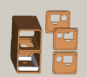
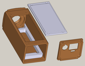
Body of camera for developers
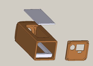
Case A consist of a large window on the top and transparent plex panel for closing. Anybody can easy modified this panel for any application.
Case B consist a large space with two bodies. Can use same as back pannel can use for backpanel plex too.
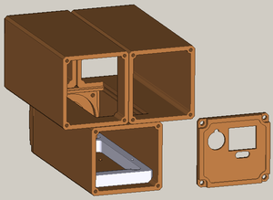
Another version of a "developer" camera body
Here are the rendered 3d-image and the source files [[1]]
