Difference between revisions of "103695"
(Created page with "==103695 - IMU Adapter Board== frame|[[Media:103695a.pdf|103695A Circuit Diagram, Parts List, PCB layout [[Media:103695a_gerber.tar...") |
|||
| Line 1: | Line 1: | ||
==103695 - IMU Adapter Board== | ==103695 - IMU Adapter Board== | ||
[[Image:103695.jpeg|frame|[[Media:103695a.pdf|103695A Circuit Diagram, Parts List, PCB layout]] [[Media:103695a_gerber.tar.gz|103695A Gerber files]]]] | [[Image:103695.jpeg|frame|[[Media:103695a.pdf|103695A Circuit Diagram, Parts List, PCB layout]] [[Media:103695a_gerber.tar.gz|103695A Gerber files]]]] | ||
| + | === Description === | ||
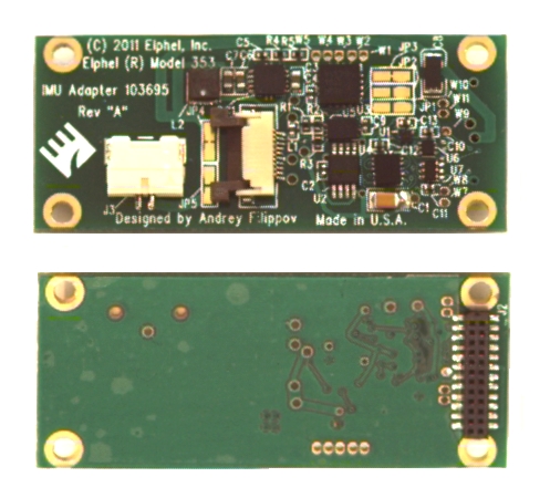
103695 is an adapter board used with the [[10369]] board to connect [http://www.analog.com Analog Devices] inertial measurement units (IMU) such as ([http://www.analog.com/en/mems-sensors/imu/adis16375/products/product.html ADIS-16375], [http://www.analog.com/en/mems-sensors/inertial-sensors/adis16405/products/product.html ADIS-16405] and similar to the [[353 | Elphel Model 353 camera]]. | 103695 is an adapter board used with the [[10369]] board to connect [http://www.analog.com Analog Devices] inertial measurement units (IMU) such as ([http://www.analog.com/en/mems-sensors/imu/adis16375/products/product.html ADIS-16375], [http://www.analog.com/en/mems-sensors/inertial-sensors/adis16405/products/product.html ADIS-16405] and similar to the [[353 | Elphel Model 353 camera]]. | ||
| + | |||
| + | Adapter uses two general purpose I/O of the camera FPGA, available on each of the [[10369]] USB/extension connectors J9..J11. The 103695 board provides 3.3V/5.0V power to the IMU (selectable by on-board resistors) and supports different speed SPI interface to the sensor unit. The device connector (J2) can accommodate a number of Analog Devices units, it should be possible to use the board with connector adapter with other SPI sensors. | ||
| + | |||
| + | Camera interface to the 103695 board is implemented in the FPGA (starting with firmware revision 8.1.0). Up 28 different 16-bit registers (plus 8 bytes of the timestamp with 1 microsecond resolution) are periodically addressed, read and stored in the camera system memory over the DMA channel. The logged register addresses are programmed at run time in the FPGA using the device driver. | ||
=== Connectors === | === Connectors === | ||
| + | ---- | ||
| + | |||
| + | ==== J1 - to 10369 board ==== | ||
| + | {| class="wikitable" style="background:#fcfcfc; " border="1" | ||
| + | |+ connector to the 10369 board | ||
| + | |- | ||
| + | ! Pin !! Signal !! Notes | ||
| + | |- | ||
| + | | 1 || VP33IN || +3.3V power input | ||
| + | |- | ||
| + | | 2 || MISO || output to the FPGA (multiplexed data/ready from SPI) | ||
| + | |- | ||
| + | | 3 || NMISO || composite input from the FPGA, source of SPI output signals | ||
| + | |- | ||
| + | | 4 || SDA || i2c SDA | ||
| + | |- | ||
| + | | 5 || SCL || i2c SCL | ||
| + | |- | ||
| + | | 6 || GND || | ||
| + | |- | ||
| + | | 7 || VP5IN || USB +5V power, not used | ||
| + | |- | ||
| + | | 8 || DM || USB data - , not used | ||
| + | |- | ||
| + | | 9 || DP || USB data + , not used | ||
| + | |- | ||
| + | | 10 || GND || | ||
| + | |- | ||
| + | |} | ||
---- | ---- | ||
Revision as of 13:30, 8 July 2011
103695 - IMU Adapter Board
Description
103695 is an adapter board used with the 10369 board to connect Analog Devices inertial measurement units (IMU) such as (ADIS-16375, ADIS-16405 and similar to the Elphel Model 353 camera.
Adapter uses two general purpose I/O of the camera FPGA, available on each of the 10369 USB/extension connectors J9..J11. The 103695 board provides 3.3V/5.0V power to the IMU (selectable by on-board resistors) and supports different speed SPI interface to the sensor unit. The device connector (J2) can accommodate a number of Analog Devices units, it should be possible to use the board with connector adapter with other SPI sensors.
Camera interface to the 103695 board is implemented in the FPGA (starting with firmware revision 8.1.0). Up 28 different 16-bit registers (plus 8 bytes of the timestamp with 1 microsecond resolution) are periodically addressed, read and stored in the camera system memory over the DMA channel. The logged register addresses are programmed at run time in the FPGA using the device driver.
Connectors
J1 - to 10369 board
| Pin | Signal | Notes |
|---|---|---|
| 1 | VP33IN | +3.3V power input |
| 2 | MISO | output to the FPGA (multiplexed data/ready from SPI) |
| 3 | NMISO | composite input from the FPGA, source of SPI output signals |
| 4 | SDA | i2c SDA |
| 5 | SCL | i2c SCL |
| 6 | GND | |
| 7 | VP5IN | USB +5V power, not used |
| 8 | DM | USB data - , not used |
| 9 | DP | USB data + , not used |
| 10 | GND |
