Mcontr: Difference between revisions
Jump to navigation
Jump to search
No edit summary |
No edit summary |
||
| Line 1: | Line 1: | ||
==Description== | ==Description== | ||
FPGA module that controls reads and writes between FPGA and DDR SDRAM (boards 10353 & 10359). | FPGA module that controls reads and writes between FPGA and DDR SDRAM (boards 10353 & 10359). | ||
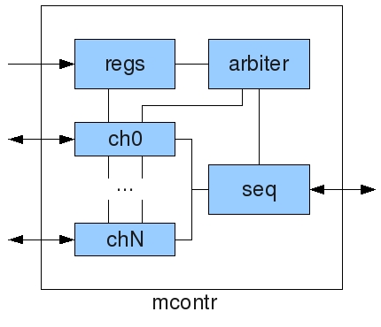
[[Image:Mcontr scheme.jpg|center|frame|[[Media:Mcontr scheme.jpg|Fig.1 Mcontr functional scheme]]]] | |||
==Bank interleaving== | ==Bank interleaving== | ||
| Line 10: | Line 12: | ||
[[Image:Bank interleaving.jpg|center|frame|[[Media:Bank interleaving.jpg|Fig. | [[Image:Bank interleaving.jpg|center|frame|[[Media:Bank interleaving.jpg|Fig.2 Bank interleaving example]]]] | ||
==Programmable SDRAM sequence== | |||
==TODO== | ==TODO== | ||
*bank interleaving | *bank interleaving | ||
*run-time programmable SDRAM sequencing | *run-time programmable SDRAM sequencing | ||
Revision as of 16:09, 18 September 2008
Description
FPGA module that controls reads and writes between FPGA and DDR SDRAM (boards 10353 & 10359).

Bank interleaving
- Taken from Theora's code.
- Banks addresses (SDA[14:13]) and order used in a single memory access: 00&10, 11&01, 10&00, 01&11.
- Both banks are opened in the beginning of the sequence.
- Write/read sequence is divided by 2 and all column addresses are the same.
- Row address of the second bank in a sequence is the first bank's + 1.


Programmable SDRAM sequence
TODO
- bank interleaving
- run-time programmable SDRAM sequencing