Difference between revisions of "10359 fix"
(→Description) |
(→2) |
||
| Line 10: | Line 10: | ||
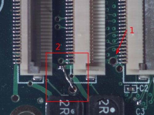
* Connect the hole to the trace on the image. | * Connect the hole to the trace on the image. | ||
====2==== | ====2==== | ||
| − | * With a 1mm drill isolate the top layer trace from the other layers. The top layer trace should not be cut. | + | * With a 1mm drill isolate the top layer trace from the other layers. The top layer trace should not be cut. If the connection on the top layer will be accidentally broken, it is possible to restore it with a wire bridge on a top layer |
Revision as of 18:18, 3 August 2010
Contents
[hide]Description
There was a design error discovered in the 10359 & 10359A boards - due to a wrong source the sensors connected to J2, J3, J4 were powered from the 10359's 2.5V instead of the correct 3.3V coming from 10353. Because of that the linear regulators on the sensor board could not maintain nominal output voltage (2.5V, 2.8V) and isolate the analog from the digital supplies. Sensor did great job operating in such conditions in such a way that image deterioration was almost not noticeable - very faint vertical stripes with a 4-pixel period on a 10338D board. Older 10338A used different linear regulators and output voltage was slightly higher, so no vertical stripes were visible (but we would still recommend to replace (or fix 10359 boards as the noise level can be reduced when applying correct power).
The fix should be applied to all 10359 & 10359A boards.
ToFix
1
- Connect the hole to the trace on the image.
2
- With a 1mm drill isolate the top layer trace from the other layers. The top layer trace should not be cut. If the connection on the top layer will be accidentally broken, it is possible to restore it with a wire bridge on a top layer
