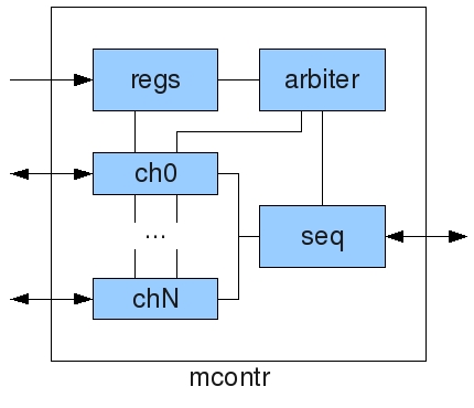
Mcontr
From ElphelWiki
Description
FPGA module that controls reads and writes between FPGA and DDR SDRAM (boards 10353 & 10359).

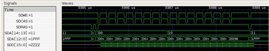
Bank interleaving
- Taken from Theora's code.
- Banks addresses (SDA[14:13]) and order used in a single memory access: 00&10, 11&01, 10&00, 01&11.
- Both banks are opened in the beginning of the sequence.
- Write/read sequence is divided by 2 and all column addresses are the same.
- Row address of the second bank in a sequence is the first bank's + 1.

Programmable SDRAM sequence
Programmable:
- sequence length
- tile length in column(x4 banks)
- tile width in rows
- address shift in a column for a new tile
- address shift in a row for a new tile
- maximum number of tiles in a column
- maximum number of tiles in a row
| Reg | Name | Description |
| 0x0c | ch0x | channel 0 tile length |
| 0x14 | ch0y | channel 0 tile width |
| 0x0d | ch1x | channel 1 tile length |
| 0x15 | ch1y | channel 1 tile width |
TODO
- bank interleaving
- run-time programmable SDRAM sequencing